Sub Dollar Time to Digital Converter: Measuring Nanoseconds
By reverse-engineering the Configurable Logic Block, it’s possible to precisely place logic to measure nanosecond delays without external components, for under a dollar!
Contents
Introduction
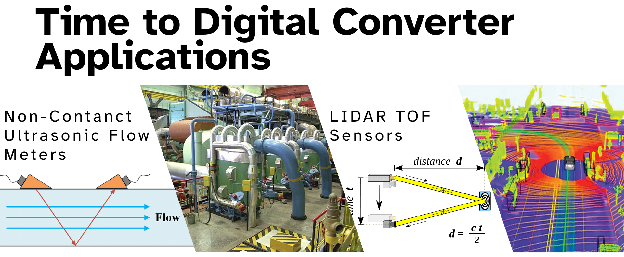
What are Time to Digital Converters?
A Time to Digital Converter (TDC) measures very small time intervals, often down to billionths of a second (nanoseconds), and converts them into digital values. You can think of it like a stopwatch for events happening too fast for ordinary electronics to track. Time to Digital Converters are used when timing matters more than anything else, such as in LIDAR, particle physics, or ultrasound imaging.
Why Do We Need Time to Digital Converters?
Time to Digital Converters are essential anywhere extremely precise timing is needed.
For example, ultrasonic flow meters can measure how fast water flows through a pipe without ever touching it. They do this by timing how long it takes a sound pulse to travel upstream and downstream. But because sound travels through water at over 3000 miles per hour, even small differences in flow require time resolution in the billionths of a second (nanoseconds) or even trillionths of a second (picoseconds).
This kind of non-invasive, high-precision sensing is critical for infrastructure applications like nuclear power plants and ultra-power-dense AI data centers, where reliable fluid monitoring is essential to cooling and safety systems. These are both examples of critical infrastructure, where failure is not an option.
Time to Digital Converters are also central to LIDAR systems, where each billionth of a second corresponds to about a foot of distance. That kind of precision enables self-driving cars to “see” their surroundings.
In addition, TDC converters are used in many, applications like:
-
Positron Emission Tomography (PET) scanners; used for cancer detection
-
Quantum Key Distribution (QKD) links; for securing data center communication
How do Time to Digital Converters Work?
Imagine you are trying to measure how long a ball stays in the air after you throw it up. You glance at a clock to time it, but what if it lands between two seconds? You can only estimate the time based on how fast the clock updates.
The same problem applies in digital systems. On a microcontroller like the PIC16F13145, the primary way to measure a time delay is by counting clock cycles with a timer. The accuracy of this method is limited by the speed of the clock.
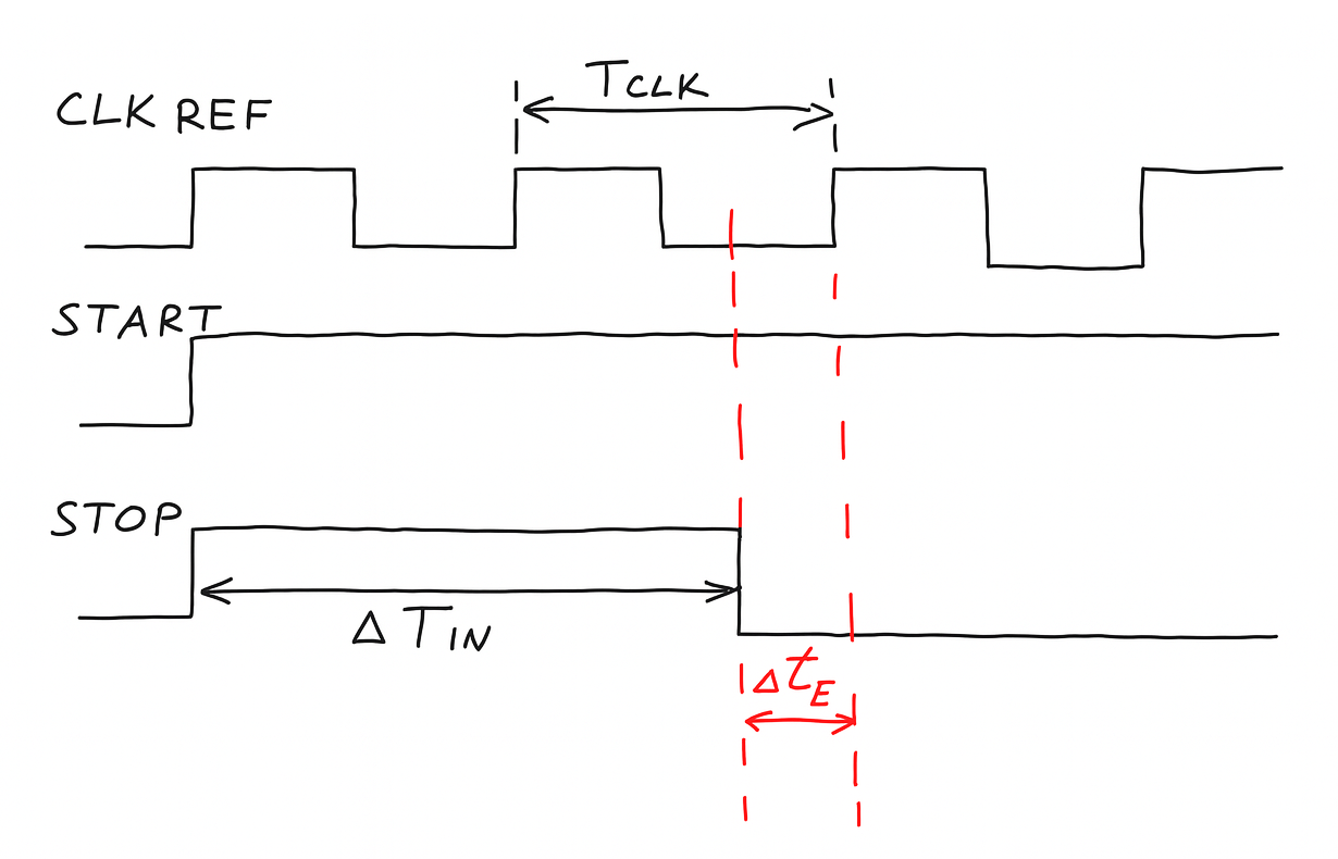
On the PIC16F13145, the fastest available clock runs at 32 MHz (OS20), which gives a minimum measurable step of 1 divided by 32 million, or 31.25 nanoseconds. Any event that happens between clock edges is effectively invisible to the timer. The uncertainty between one clock edge and the next is our timing error, written as Δtₑ.
A Time to Digital Converter improves this by measuring that “in-between” part — the small leftover time that a regular timer misses. We split the total time into two parts:
-
Coarse Time: the large steps measured by the main system timer
-
Fine Time: the smaller fractional delay that occurs between clock edges
Our goal is to find a way to measure the Fine Time as accurately as possible.
Methodology
Coarse Time
The first step is to figure out how to measure Coarse Time, the large-scale part of the delay that spans multiple full clock cycles.
Initially, I looked at the Capture Compare Modules in capture mode. These modules timestamp incoming events relative to a timer. In theory, we could use two of them, one to capture the start signal, and one for the stop signal. If we run the timer from the HFINTOSC at its maximum 32 MHz, we get coarse timing steps of 31.25 nanoseconds.
However, during testing, I noticed that all captured times were in increments of 4 clock cycles: 4, 8, 12, and so on. After double-checking the datasheet, I found a key detail I had missed:
“Clocking Timer1 from [FOSC] must not be used in Capture mode. For Capture mode to recognize the trigger event […] Timer1 must be clocked from [FOSC/4].”
This meant I could not use the full 32 MHz resolution in capture mode. So I went back to the drawing board.
While reviewing the datasheet, I noticed that Timer1 supports gate control. This allows the timer to be enabled only while a control signal is active. What I really wanted was to run the timer only when the start signal is high and the stop signal is low. This is a simple XOR condition.
By wiring the start and stop signals into a Basic Logic Element (BLE) and configuring it as an XOR gate, I was able to use that as the gate input for Timer1. The timer now runs only for the duration between the two events.
With this setup, I initialize the timer to 0 before the event. When the event ends, I simply read the Timer1 register to get the coarse delay. At that point, I can move on to measuring the fine delay.
Fine Time
This is where things get interesting. One of the most common ways to measure sub-clock timing is to use a Tapped Delay Line.
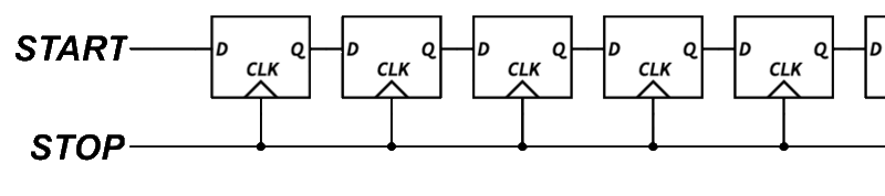
A tapped delay line is a series of logic elements that each introduce a small propagation delay. If each element delays the signal by 1 nanosecond, and the signal passes through several of them before being sampled, we can estimate the fine time by counting how far the signal got.
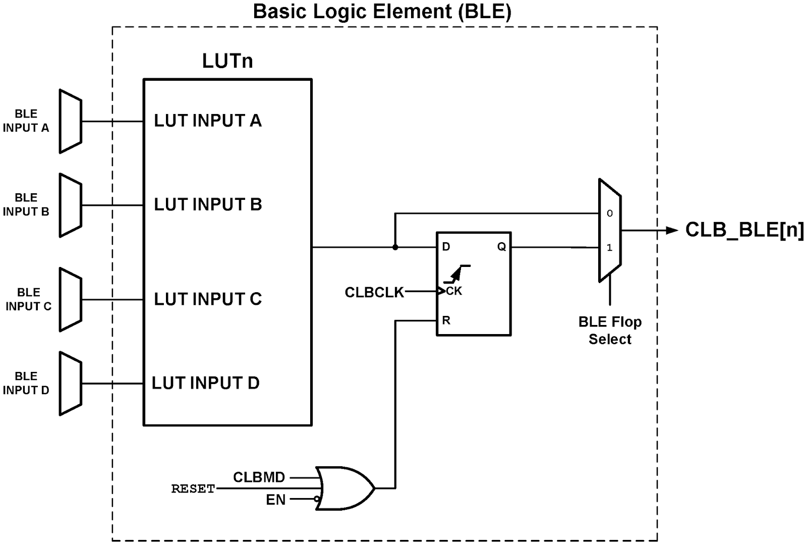
To build this, we need transparent latches, logic elements that pass their input through when a control signal is low, and hold their state when it is high. Unfortunately, the output flops inside each BLE in the Configurable Logic Block (CLB) do not support transparent mode.
To implement the delay line, we need lower-level control of the BLE behavior than what the CLB toolchain allows.
Going Deeper; Reverse Engineering the CLB
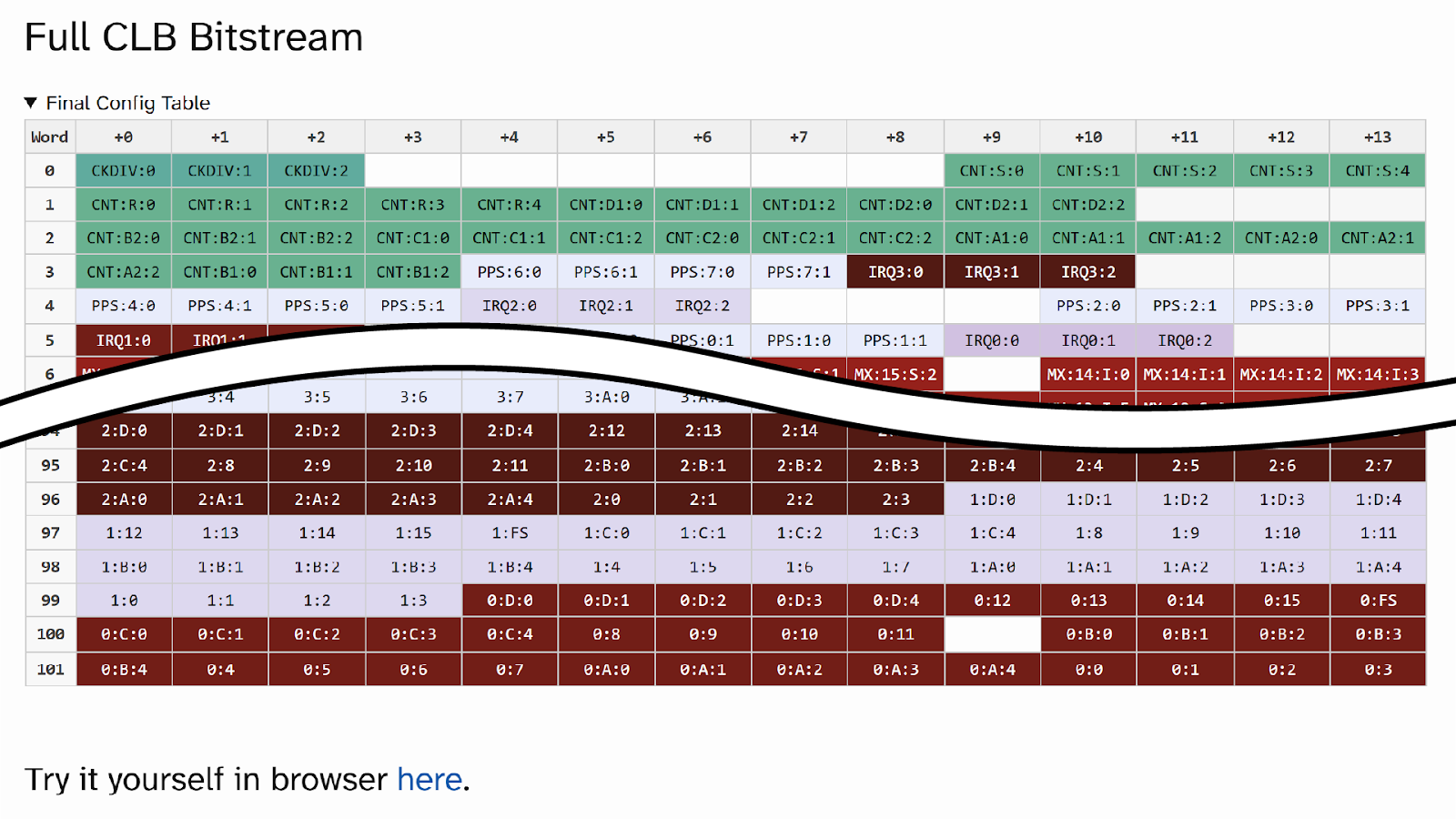
After working with the CLB Synthesizer for a while, it became clear that the tool did not provide the level of control I needed, especially for precise logic placement. So I decided to reverse engineer the CLB myself.
I started by analyzing the datasheet alongside the output of the CLB Synthesizer. By feeding carefully crafted Verilog designs into the toolchain and inspecting the resulting bitstreams, especially the intermediate .fasm files, I was able to correlate high-level constructs like LUT configurations and input mux selections to individual bits in the raw configuration.
To streamline the process, I built Python tooling to automate delta comparisons and track correlations across multiple design variants. This helped isolate how each part of the logic was encoded, one field at a time.
As the reverse engineering progressed, I expanded the scope to include BLE interconnects, FLOPSEL control, clock division, and input/output muxing. Eventually, I developed what I believe is a complete model of the CLB bitstream format. The hardest part was forcing the synthesizer to preserve specific BLE placements without optimizing them away, I solved this by generating randomized but valid logic layouts that preserved structure while varying details.
With the model in place, I wrote Python tools to generate, edit, and visualize bitstreams directly.
You can read the full details here. You can even build and visualize CLB bitstreams directly in your browser (no backend required) here.
Illegal Logic; Building the TDC Core
To implement a transparent latch in a Basic Logic Element (BLE), we need to build logic that passes the input to the output when a control signal is low, and holds the output when the control is high, effectively creating a gated pass-through with inherent delay.
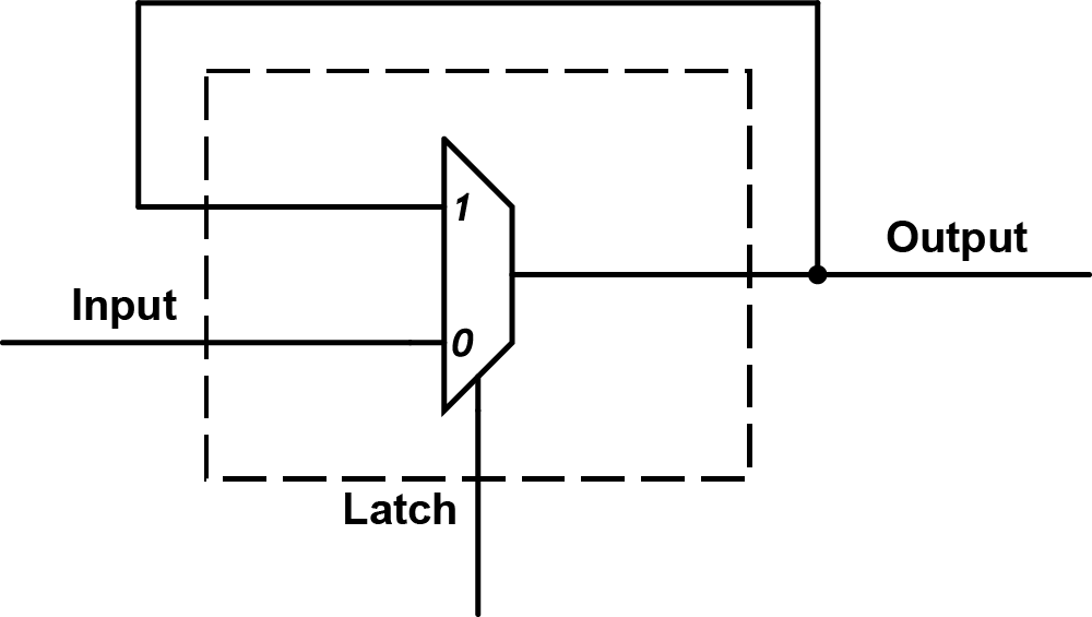
The digital designers among you will have horrified expressions, unclocked or “transparent” latches are typically prohibited because they can introduce unpredictable behavior due to propagation delays and race conditions. But here, that delay is exactly what we want.
We can use the BLE’s Look Up Table (LUT) to implement the required logic. However, we immediately run into a structural limitation: the BLE input architecture.
Inputs to BLEs are divided into four banks:
- Bank A: BLE0 through BLE7
- Bank B: BLE8 through BLE15
- Bank C: BLE16 through BLE23
- Bank D: BLE24 through BLE31
Each BLE can only connect to specific input banks. For example, if we are working in BLE4 (part of Bank A), and we want to take feedback from BLE3 (also in Bank A), we run into a problem: both source and destination are restricted to the same input path. There is no way to connect BLE3 to BLE4 through the same bank.
To resolve this, we must alternate between banks as we build our delay chain, switching input sides to avoid conflicts and maintain the desired feed-forward path.
How many stages do we need?
The datasheet provides only limited information about the propagation delay of a Basic Logic Element (BLE), just a typical value of 10 nanoseconds (CLB01).
Thanks to the reverse engineering work described earlier, I had full control over BLE placement and interconnect routing. This made it possible to build a precisely structured delay line, chaining BLEs end to end with known topology. I then moved the output tap back one BLE at a time to measure the delay introduced by each stage. Here are the results:
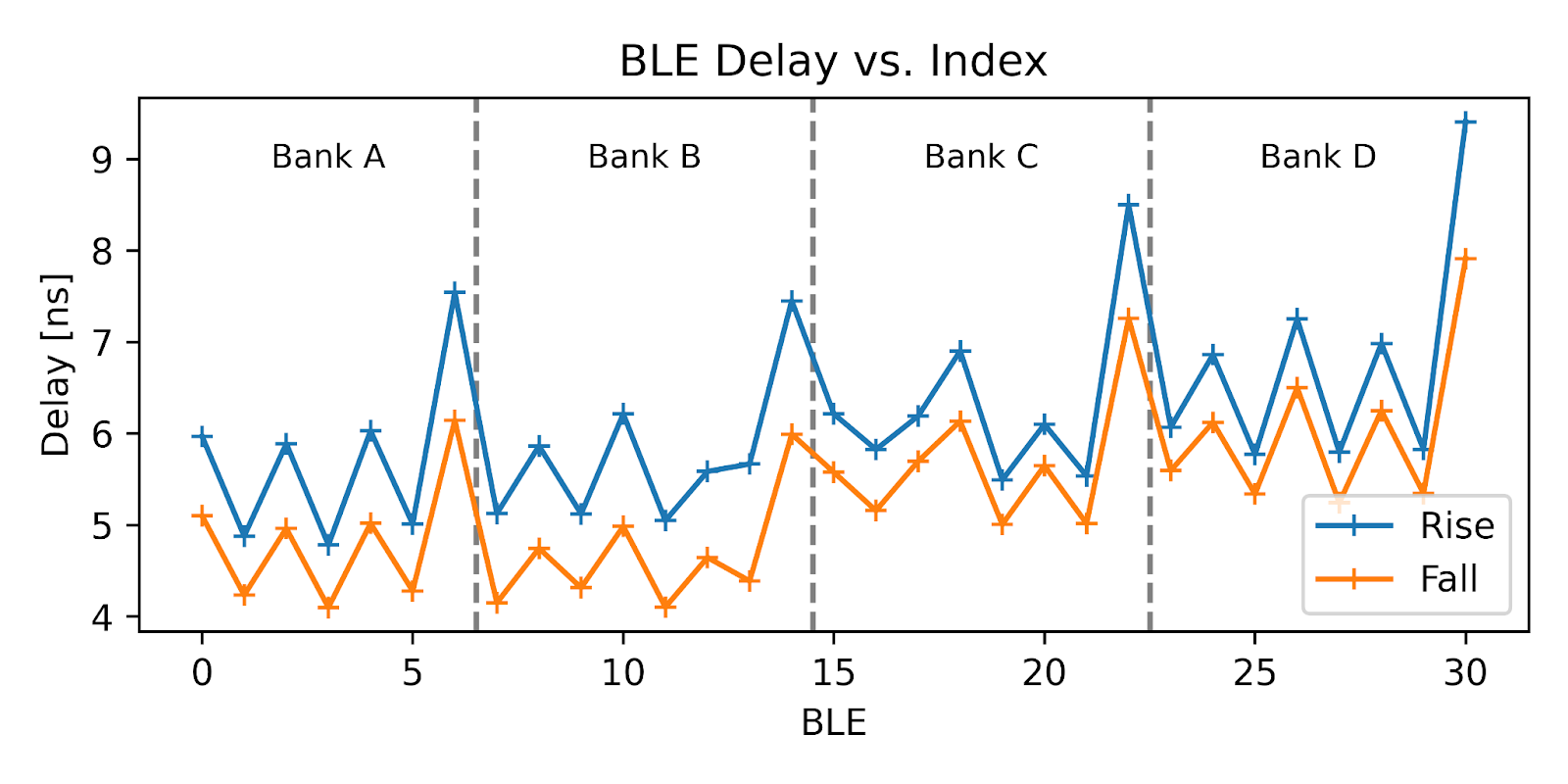
The measurements revealed noticeable jumps in delay at bank boundaries — this is due to inter-bank routing overhead. On average, I measured:
-
5.8 nanoseconds of delay for rising edges
-
5.1 nanoseconds for falling edges
These values are roughly half of the datasheet’s nominal 10 ns, with an additional ~2 nanoseconds of delay every time the signal crosses a bank boundary.
Because of the way BLE input banks are organized, each stage in the tapped delay line must alternate between banks. As a result, we incur the bank delay on every connection. Given the 31.25 ns clock period at 32 MHz, this means we can fit about four BLE stages per cycle, giving us a fine resolution of approximately 8 nanoseconds per tap.
What do we actually measure?
To measure fine time, we need to know exactly how close the STOP signal was to the next clock edge, the part the coarse timer cannot resolve. To get that, we take advantage of a flexible feature of the CLB: programmable input synchronization.
Each CLB input can be configured independently to pass through a two-stage synchronizer, which delays the signal until it is safely aligned to the internal CLB clock. Alternatively, synchronization can be bypassed entirely, allowing the input to propagate immediately into the logic.
This flexibility is key. We configure the STOP signal to enter the CLB along two different paths:
-
One path goes directly to the delay line without synchronization
-
The other is routed through the synchronized input path
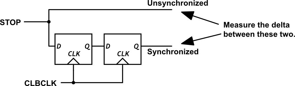
The unsynchronized path captures the STOP signal immediately, letting it begin propagating through the TDC delay line. Meanwhile, the synchronized version is held until the next clock edge (or two, depending on mode). By comparing these two signals, one raw, one delayed, we can infer how much fine time was left before the next coarse timer tick.
This only works because the CLB allows flexible control over each input’s synchronization behavior. The reverse engineering gave us the exact configuration bits needed to route signals this way, and to do so deterministically.
In effect, we are measuring the gap between an unsynchronized event and its synchronized copy. That gap is the fineΔtₑ time we are trying to resolve.
Increased TDR Resolution
How can we improve the resolution of our Time to Digital Converter beyond the delay per BLE? One way is to make an interleaved measurement, using two parallel TDC chains offset in time by half a stage. This gives us finer timing granularity. But how do you delay one chain by half a BLE, when BLEs are discrete logic elements?
The answer lies in the CLB’s input multiplexer architecture, and in the small imperfections that exist in real hardware.
Each of the CLB’s 16 input channels (IN0 to IN15) can be independently connected to one of 29 signal sources, including PPS pins, timer outputs, and other internal elements. These IN channels are then available to every BLE in the fabric. However, due to physical layout, the routing delay for each IN channel is not exactly the same. In digital design, this variation is called skew.
To measure this, I manually configured all 16 IN channels to receive the same PPS pin, then connected them one at a time to the same BLE. By measuring the propagation delay through the BLE as I changed the input selection, I was able to characterize the skew introduced by each input path.
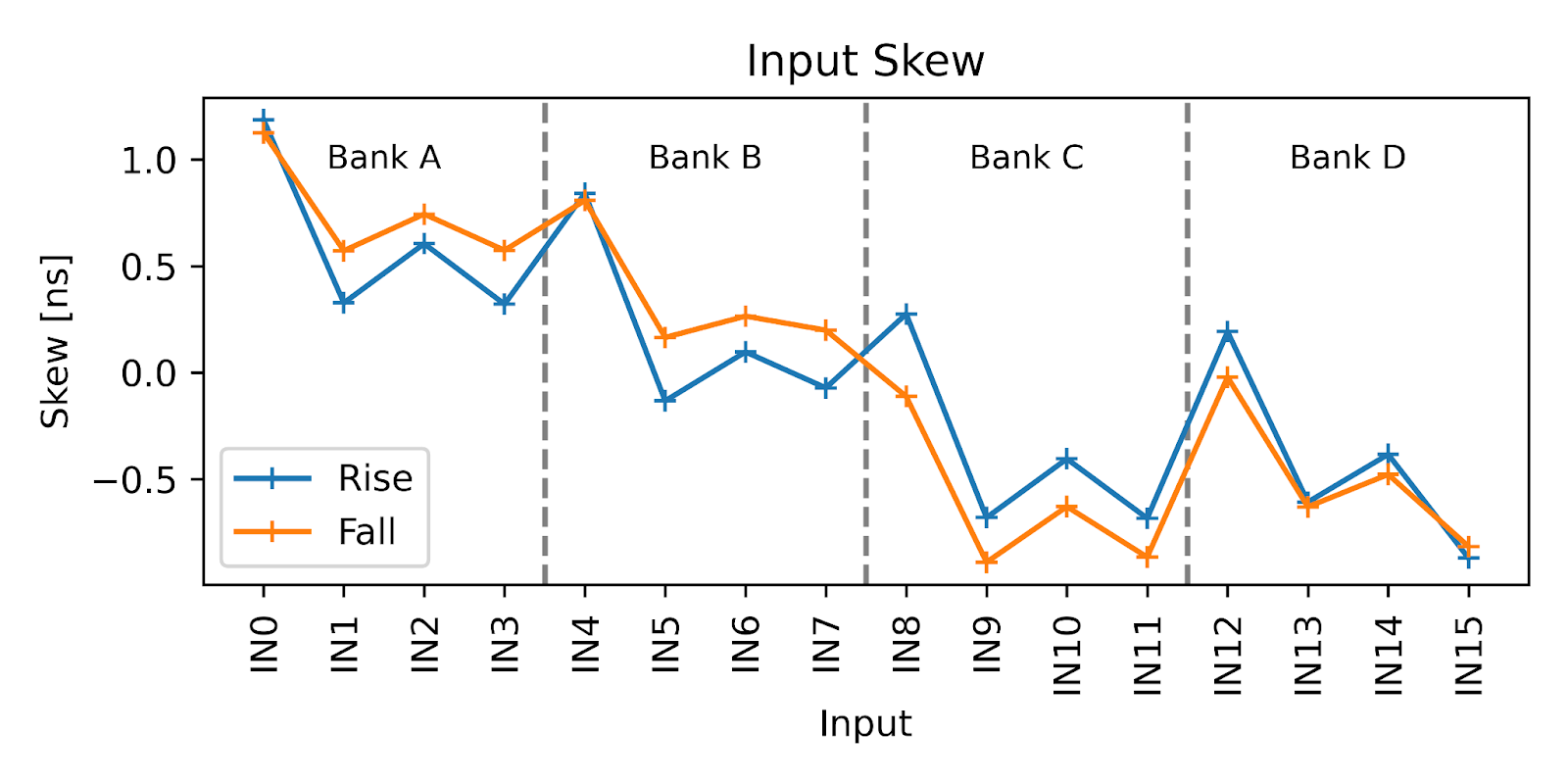
As you can see, the input skew across the IN channels is remarkably small. Clearly, Microchip took care in the physical layout of the input network. Still, there are measurable variations caused by routing differences, wire length mismatches, drive strength, and internal buffering.
By carefully selecting which IN channel drives each BLE in the delay chain, we can fine-tune the timing offset at sub-BLE resolution. This lets us interleave two TDC chains with a phase offset, effectively doubling the resolution of our time measurement.
In practice, I created a 4-stage delay line, then built a second line with identical logic and placement, but offset each BLE’s input to use a slightly more delayed IN channel. The result is a pair of interleaved TDCs that, when combined, produce timing resolution finer than any individual stage.
This level of control is only possible because we can manually configure, place, and route every detail of the design.
Details
Recall that the CLB input synchronizer introduces a delay of two clock cycles. This means the unsynchronized signal needs to be held off until the synchronized version has passed through. To do this, we insert a few buffer BLEs before the TDC core to slow the signal just enough. This ensures both signal paths line up when sampling begins.
The next issue is how to read the result. The only supported way to get signals out of the CLB is through the PPS outputs. In Revision B of the datasheet, Microchip documented a SWOUT register that was supposed to allow reading CLB outputs directly. I tested this by trying every access method described, including direct read and latched modes, but always received all zeros.
In later revisions, Microchip removed any mention of SWOUT from the datasheet. The Revision C change note states: “Removes references to CLB registers that are no longer user-accessible.” There was no errata entry documenting the removal or indicating that it was a known issue.
I would love to see this work in the future on this part or another! Or at least more detailed errata.
Putting it all Together
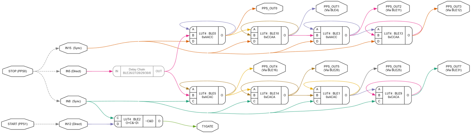
Here is the final CLB layout. It includes two interleaved TDC chains, each driven by skewed inputs to achieve half-stage offsets. There is also a one-cycle delay for synchronizer alignment, and an XOR gate implemented in a BLE to drive the timer gate input.
Below is the core readout function. It resets the timer, waits for the STOP signal, samples the coarse and fine values, and returns the final delay:
uint24_t tdc_read(void)
{
    TMR1_Write(0u);                // reset coarse timer
    TRIG_OUT_SetHigh();            // START
    while (!TRIG_IN_GetValue()){
        if (TMR1_Read() > TIMEOUT){
            TRIG_OUT_SetLow();     // clean up
            return 0;
        }
    }

    __delay_us(2); // latch input

    uint16_t coarse_ticks = TMR1_Read();

    // thermometer code B string
    uint8_t b = CPPS0_GetValue() + CPPS1_GetValue()
              + CPPS2_GetValue() + CPPS3_GetValue();

    // thermometer code A string
    uint8_t a = CPPS4_GetValue() + CPPS5_GetValue()
              + CPPS6_GetValue() + CPPS7_GetValue();

    uint8_t fine_index = (uint8_t)(a * 5u + b);
    // coarse part in 0.125-ns units
    uint32_t ret = ((uint32_t)(coarse_ticks - LATCH_DELAY) *
                         COARSE_U_MUL) / COARSE_U_DIV;
    // add fine offset
    ret += fine_u8[fine_index] + FINE_BIAS_U;

    TRIG_OUT_SetLow();

    return (uint24_t) ret;
}
Summary of the flow
-
Reset the coarse timer
-
Wait for the STOP signal
-
Latch the TDC chains
-
Read the coarse delay from TMR1
-
Count the number of active stages in both A and B chains
-
Use a lookup table to convert that to a calibrated fine delay
-
Add the fine and coarse components
-
Return the final time (in 0.125ns LSBs)
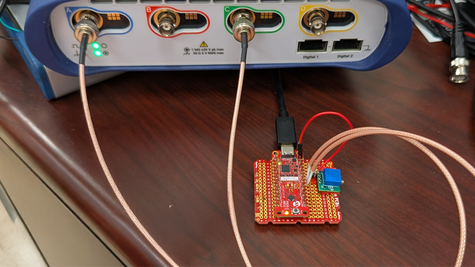
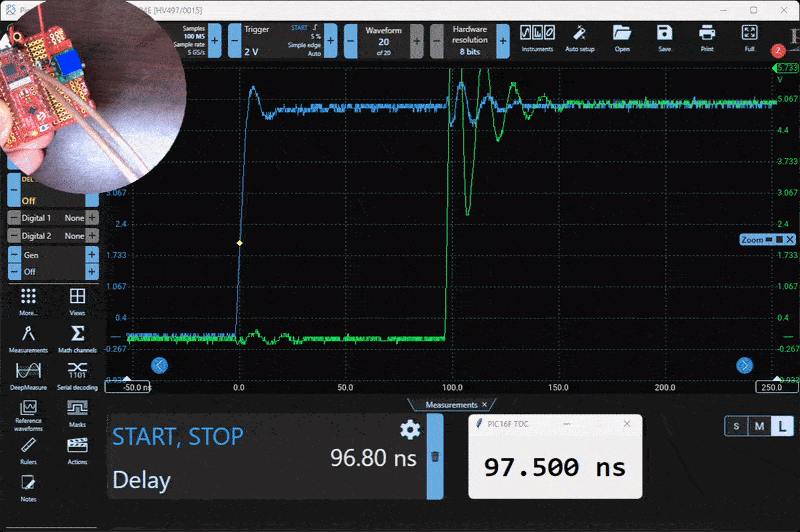
Here is the test setup. A small PCB generates a variable 0 to 300 ns delay using a 20-turn potentiometer.
Results
To test and evaluate the system, I built a simple delay generator using a resistor, a capacitor, and a logic buffer. This circuit produces a tunable delay based on the RC time constant, and it worked well for characterizing the TDC. Below is a capture from the Picoscope alongside the live serial output from the PIC.
Characterization
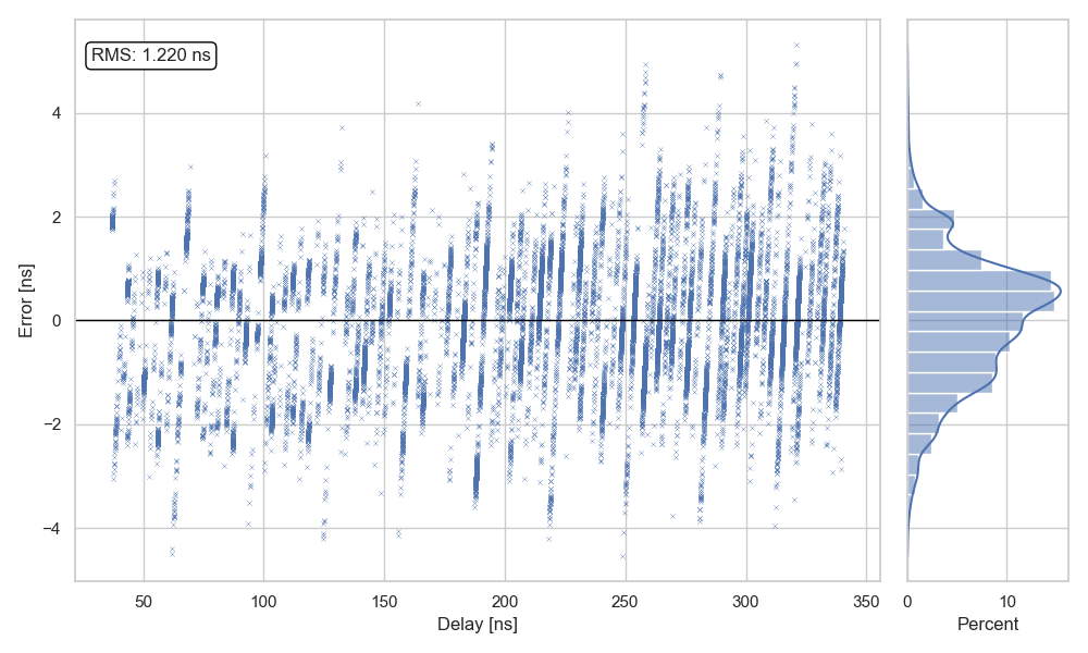
I wrote a Python script to capture and compare the output from the PIC and the Picoscope simultaneously. The goal was to quantify the measurement error. I collected around 20,000 data points across a delay range of 30 ns to 300 ns. The measured RMS error was 1.22 ns over that range.
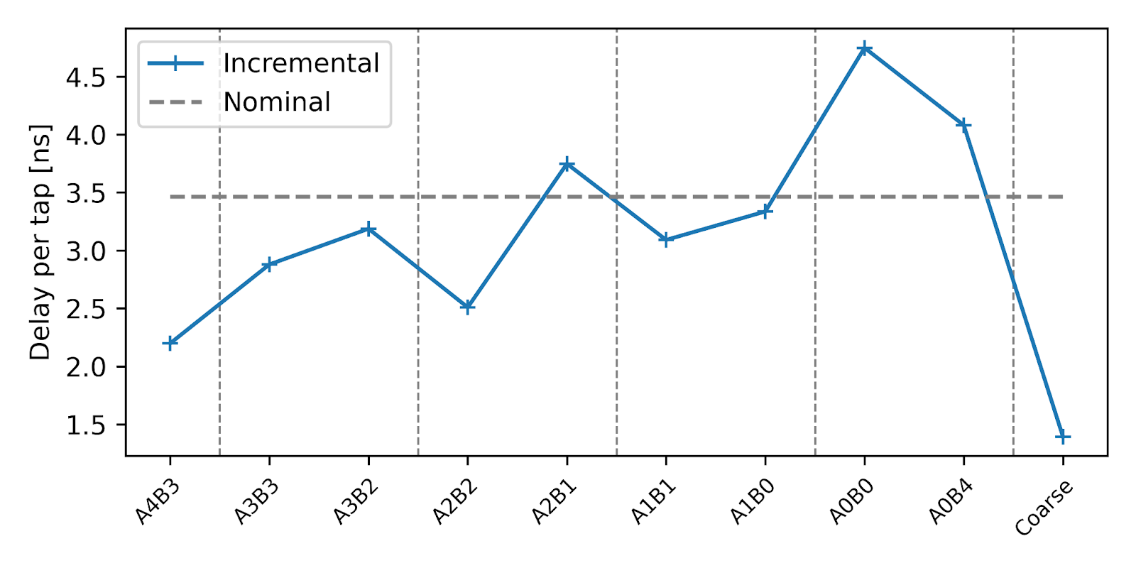
By combining the A and B TDC chains, I observed 10 unique fine codes. The tap points and their measured offsets are shown below:
| Tap | Offset [ns] | Δ [ns] |
|---|---|---|
| A4B4 | +0.0000 | +0.0000 |
| A4B3 | +2.1984 | +2.1984 |
| A3B3 | +5.0777 | +2.8793 |
| A3B2 | +8.2653 | +3.1876 |
| A2B2 | +10.7749 | +2.5096 |
| A2B1 | +14.5232 | +3.7483 |
| A1B1 | +17.6146 | +3.0914 |
| A1B0 | +20.9511 | +3.3365 |
| A0B0 | +25.6994 | +4.7483 |
| A0B4 | +29.7806 | +4.0812 |
| Coarse | +31.1745 | +1.3939 |
The table shows that tap spacing is not uniform. Below is a plot of the Incremental Tap Delay, which corresponds to the system’s Differential Nonlinearity (DNL).
The widest code is approximately 4.7 ns, which matches the observed peak error. The RMS error is about 1.2 ns for raw measurements. For time-of-flight applications, the effective error is about half the code width: around 2.4 ns peak error and 0.7 ns RMS error, assuming symmetric paths.
The measurable range spans from about 10–20 ns up to 2 milliseconds, limited by TMR2. You could extend the range by tracking timer overflow in software.
Discussion
The reason I use Microchip parts is the strength of their Core Independent Peripherals (CIPs). Even in low-cost, small-footprint devices, it’s possible to implement complex behaviors like gating, edge detection, timing, and logic sequencing, all without burdening the CPU. That capability allows small MCUs to punch well above their weight, in terms of speed, power, and capability.
The Configurable Logic Block (CLB) expands this idea dramatically. With LUTs, flops, counters, and routing fabric inside the silicon, the CLB provides a peripheral I always wish I had in Microchip microcontrollers.
What makes the CLB even more compelling is what you can do with tidal and precise control. With full access to configuration bits, it becomes possible to do unhinged things, things people told me were impossible. Transparent latches. Skew-calibrated fine timing chains. Interleaved measurement structures. Illegal logic. You are no longer limited by what the toolchain exposes, only by what the hardware can physically do.
This design takes advantage of exactly that. With complete control over placement, routing, and synchronization, it becomes possible to push the CLB into new territory. The result is not just a working Time to Digital Converter, but a demonstration of how flexible and powerful CIPs can be when used to their fullest extent.
I expect the CLB will be most useful as a black box module, where people design peripherals for users to drop into their designs and use. You could imagine IRDA RX/TX frontends for UART or a BPSK code generator, or WS2812 modulators etc. I packaged the TDC like this with the hope it will be useful.
Conclusion
Here is the final simplified block diagram of the integrated Time to Digital Converter, using nothing more than on-chip logic. Using just the Configurable Logic Block (CLB) and Timer1.
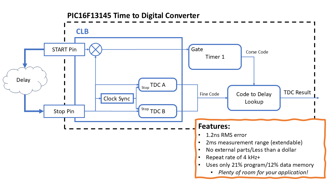
By reverse engineering the bitstream I was able to get the precise layout control I needed to
- Measures sub-clock delays with fine time resolution of ~1.2 ns RMS
- Repeat rate of over 4 kHz
- Uses only 21% of program memory and 12% of data memory
- Leaves all other peripherals free and untouched
- With no external components
The system works by splitting time measurement into coarse and fine components. Timer1 captures coarse delay, while a hand-constructed tapped delay line, made from CLB BLEs, measures fine delay with sub-stage interleaving. By exploiting skew in the input multiplexer, I doubled resolution by building interleaved TDC chains offset by physical routing mismatches.
Resources
- Drop-in CLB bitstream for PIC16F13145
- Source code for the TDC driver
- Demo with serial output
- Example project measuring delay
- Bitstream parser and generator
- BLE routing visualizer
- Try it in browser here
PS; Closing Notes
Cross Device Compatibility
I have three different Curiosity Nano dev boards from different lots and when loaded with my tuned coefficients they all have around the same errors around 1.5ns RMS 5ns peak error, dominated by HFINTOSC frequency error. Over long runs I expect you to get about the datasheet 2% HFINTOSC error (just solder down a crystle to get ppm error!) plus around 1.5ns RMS/5ns peak error for small intervals. Of course this was not a full PVT characterization your mileage will vary.
There is a lot of research about self calibrating architecture, connecting the TDC core in a loop as a free running oscillator and sampling it to get a code density plot to self calibrate out PVT drift, this is possible on this by loading an alternate cal bitstream, making a code histogram. You can do even better than some FPGA TDCs because we can guarantee exactly the same interconnect layout except for the loop.
This is left as an exercise for the reader.
What about Allan Devation/Slew Sensitivity/Deadtime/etc.
Go buy a real TDC.