No DAC? No Problem: Building a DAC in the CLB
Contents
Introduction
By pushing the CLB to its limits, it’s possible to build a sigma-delta DAC out of thin air, no external chips required.
I used the Configurable Logic Block (CLB) in the PIC16F13145 to build a 16-bit digital-to-analog converter (DAC). For less than the cost of a standalone DAC—under fifty cents—you can implement a smart, flexible, high-resolution DAC, while still retaining access to the rich set of onboard peripherals.
What is a Digital-to-Analog Converter?
A digital-to-analog converter (DAC) allows microcontrollers and other digital devices to interface with the analog world. It converts a digital value, such as a binary number representing a voltage, into a continuous analog output like a voltage or current. It serves as the counterpart to an analog-to-digital converter (ADC).
Applications: From Music to Medical Imagers to Quantum Computers
DACs are commonly used to drive audio outputs, but they also play a critical role in many other domains. Here are just a few real-world applications where a compact 16-bit DAC operating below 100 ksps is sufficient:
- Aviation: Used to drive analog actuators for regulating cabin pressure outflow valves with ±10V outputs and smooth analog control.
- Space: ESA’s Athena X-IFU relies on precision DAC outputs to stabilize cryogenic detectors to within a few millikelvin.
- Automotive: Used in adaptive suspensions to drive continuous damping control valves with ~5 kHz analog bandwidth.
- Communications: DACs drive thermal tuning loops for laser wavelength stabilization in resonator-based laser communication systems.
- Industrial: Common in 4–20 mA loop transmitters, where they generate precise analog control signals.
- Quantum Computing: Used to bias comparators in qubit readout systems for accurate threshold detection.
- Medical: Drives analog setpoints like the photomultiplier tube bias in PET scanners for cancer detection.
- Semiconductor Fabrication: Driving piezo linear actuators to position semiconductor manufacturing optics amplified from a small signal to the required 220V with a Microchip HV56022.
Methodology
Delta Sigma Digital to Analog Converters
To implement the DAC, I used the CLB to create a delta-sigma DAC. Unlike resistor ladder or PWM-based DACs, delta-sigma DACs generate a 1-bit high-speed digital output stream that is then filtered to recover a clean analog signal. This approach allows for extremely high effective resolution with minimal hardware, ideal for embedded systems.
How do we Convert Digital Pulses to Analog?
Every clock cycle, we can drive a digital output pin either high or low. By alternating states every two clock cycles, the average value is 50%. If we filter this square wave, we get an average voltage halfway between low and High.
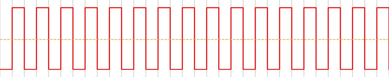
To generate more levels, we can extend this to a fixed number of samples. For example, to generate 8 discrete levels (3-bit resolution), we can take 8-cycle segments and vary how many are high (0 to 8):
This idea scales to higher resolution. For 10 bits (1024 steps), we’d need to generate and average 1024 individual high/low states per output value. But this leads to a challenge: ripple. Even with filtering, the switching noise can dominate the signal if not filtered sufficiently.
Suppose we’re using a 32 MHz clock and an 8-cycle PWM loop. That results in a 4 MHz output waveform. If we filter at 2 MHz (half the PWM frequency), the ripple is still ~60% of full scale—far too high for 8-bit accuracy. To reduce ripple to within 1 LSB (12.5% for 3 bits), we need a much lower filter bandwidth:
| Bits | FFilt/FPWM | FFilt @ FPWM (32MHz / 2ⁿ) |
|---|---|---|
| 3 | 1 to 13 | 320 kHz @ 4.00 MHz |
| 4 | 1 to 25 | 80 kHz @ 2.00 MHz |
| 6 | 1 to 100 | 5.0 kHz @ 500 kHz |
| 8 | 1 to 400 | 310 Hz @ 125 kHz |
| 10 | 1 to 1,600 | 20 Hz @ 31.2 kHz |
| 12 | 1 to 6,400 | 1.2 Hz @ 7.81 kHz |
| 14 | 1 to 26,000 | 78 mHz @ 1.95 kHz |
| 16 | 1 to 100,000 | 4.8 mHz @ 488 Hz |
For high-resolution applications (10+ bits), PWM becomes impractical—the required filter time constant becomes too long for real-world use.
Delta Sigma
How can we do better, with the same clock output? We need to make the parts of the signal we don’t want happen more frequently so they are easier to filter out. Filters work better the higher the frequency (the more often we switch).
First, we start with a system that swaps its output every clock cycle. We get feedback from the output. If the output is low then we go high, if the output is high then we go low.
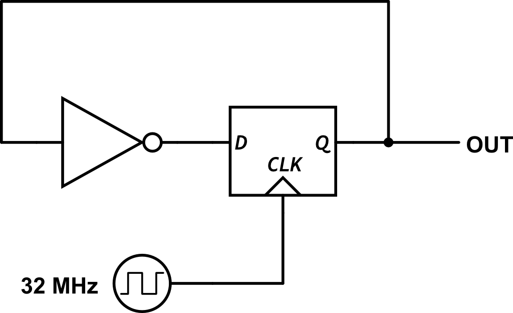
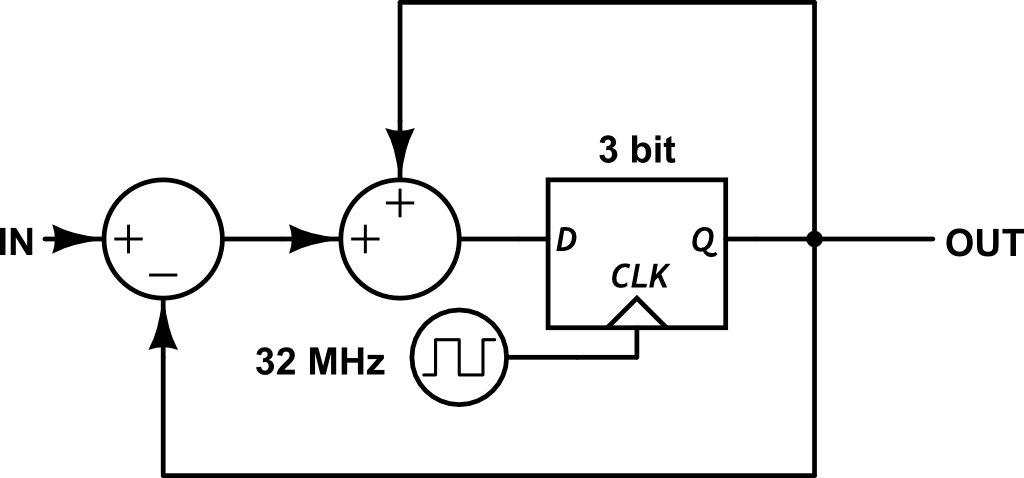
This configuration is not terribly useful. What if we want out eight outputs? The 3-bit output? We can keep track of how much output we have sent out. If we think of the 0 to 7 out as fractions of the total, as 0, 0.125, 0.25, … 1. For example we might want to output 4 * 0.125 or 0.5.
We can use a 3-bit counter to keep track of the state. And every cycle we want the output to be 4 * 0.125 or 0.5 so we add that to our tracking counter. When the counter gets so large we need to subtract full scale, we can let it roll over effectively “subtracting” full scale.
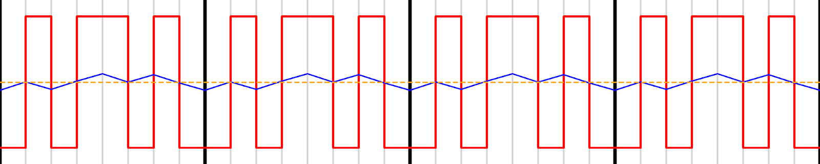
This outputs the following pattern: Vs. the 4-bit PWM pattern, it has a lot more edges, closer together. But we only need half of the filtering to get an output flat to 1 LSB; because the edges are so close to one another.
This advantage only grows as the number of bits of resolution you need grows. At 16 bits, with the same 32MHz clock, you can get over 100,000 times the bandwidth. This effect is called noise shaping, where we have as many edges as possible to push the noise to higher (easier to filter) frequencies.
| Bits | FFilt/FCLK | FFilt @ FCLK | BW gain vs PWM |
|---|---|---|---|
| 3 | 1.3e−1 | 4.2 MHz | 13 |
| 4 | 6.3e−2 | 2.0 MHz | 25 |
| 6 | 1.6e−2 | 510 kHz | 100 |
| 8 | 3.9e−3 | 120 kHz | 400 |
| 10 | 9.8e−4 | 31 kHz | 1,600 |
| 12 | 2.4e−4 | 7.7 kHz | 6,400 |
| 14 | 6.1e-5 | 2.0 kHz | 26,000 |
| 16 | 1.5e−5 | 480 Hz | 100,000 |
Implementation
The CLB in the PIC16F13145 provides 32 LUTs. To implement a 16-bit sigma-delta DAC, we use those LUTs to build a 16-bit accumulator. The beauty of delta-sigma is that we don’t need an explicit comparator or overflow logic—letting the accumulator wrap around naturally performs the necessary subtraction. The carry bit becomes our 1-bit DAC output.
Because each adder stage requires both a sum and a carry output, each bit consumes two LUTs. That allows a 16-bit accumulator in 32 LUTs maxing out the CLB’s capacity.
Verilog Reference Model
Here’s a simple Verilog implementation of the accumulator-based delta-sigma DAC:
module dac_16 (

    input        clk,          // bit-stream clock

    input [15:0] din,          // 16-bit input word

    output       out           // 1-bit ΣΔ output

);

    reg [15:0] acc;

    reg        carry;

    always @(posedge clk) begin

        {carry, acc} <= acc + din;

    End

    assign out = carry;

endmodule
And thanks to Verilog blocks, you can drop it right into the CLB Synthesizer (project file).
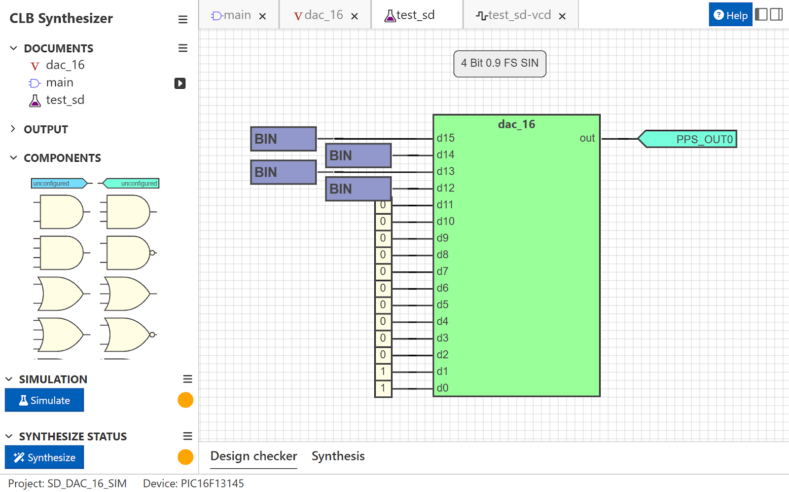
Now you can even simulate the design!
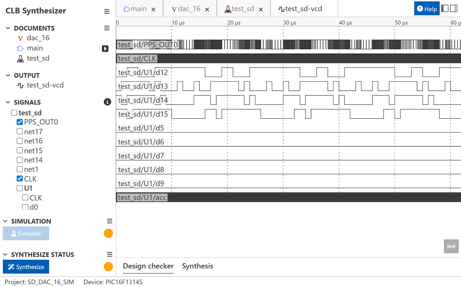
Unfortunately this design is too complex to synthesize in CLB Synthesizer (it can only handle about 40-60% full; not 100% full). But thanks to my reverse engineering I can manually synthesize it!
from itertools import cycle

from pathlib import Path


from bitstream import Bitstream

from build_lut import LUT4, a, b, c, d

from clb_graph import generate_dot_from_config

from data_model import (_CLB_ENUM, BLE_CFG, BLEXY, FLOPSEL, LUT_IN_A, LUT_IN_B,

                        LUT_IN_C, LUT_IN_D, PPS_OUT_NUM, CLKDIV)


BANKS = {"A": LUT_IN_A, "B": LUT_IN_B, "C": LUT_IN_C, "D": LUT_IN_D}

NAME2BANK = {n: k for k, v in BANKS.items() for n in v.__members__}

SYM = {"A": a, "B": b, "C": c, "D": d}


ble = lambda i: (LUT_IN_A, LUT_IN_B, LUT_IN_C, LUT_IN_D)[i // 8][f"CLB_BLE_{i}"]

swin = lambda i: (LUT_IN_A, LUT_IN_B, LUT_IN_C, LUT_IN_D)[i // 8][f"CLBSWIN{i}"]


bs = Bitstream()


# BLE indices grouped by bank

luts = {b: [i for i in range(32) if NAME2BANK[ble(i).name] == b] for b in "ABCD"}


carry_cycle = cycle("CD")

stages = {

    i: (

        luts["B" if i < 8 else "A"].pop(0),  # SUM LUT

        luts[next(carry_cycle)].pop(0),

    )  # CARRY LUT

    for i in range(16)

}


for bit, (sum_lut, car_lut) in stages.items():

    d_in = swin(bit)

    s_fb = ble(sum_lut)

    taps = [d_in, s_fb] if bit == 0 else [d_in, s_fb, ble(stages[bit - 1][1])]


    va, vb, *vc = [SYM[NAME2BANK[t.name]] for t in taps]  # symbols

    sum_expr = va ^ vb if bit == 0 else va ^ vb ^ vc[0]

    carry_expr = va & vb if bit == 0 else (va & vb) | (vb & vc[0]) | (va & vc[0])


    kws = {f"LUT_I_{NAME2BANK[t.name]}": t for t in taps}

    bs.LUTS[BLEXY(sum_lut)] = BLE_CFG(

        LUT_CONFIG=LUT4(sum_expr).bitstream(), FLOPSEL=FLOPSEL.ENABLE.value, **kws

    )

    bs.LUTS[BLEXY(car_lut)] = BLE_CFG(

        LUT_CONFIG=LUT4(carry_expr).bitstream(),

        FLOPSEL=FLOPSEL.ENABLE.value if bit == 15 else FLOPSEL.DISABLE.value,

        **kws,

    )


# Final sigma‑delta output

fin = stages[15][1]

grp = fin // 4

bs.PPS_OUT[PPS_OUT_NUM[grp]].OUT = _CLB_ENUM[grp](fin % 4)

print(repr(_CLB_ENUM[grp](fin % 4)))

print(generate_dot_from_config(bs))
Here is the graph (it’s very wide, basically a 32 BLE long chain):

Results
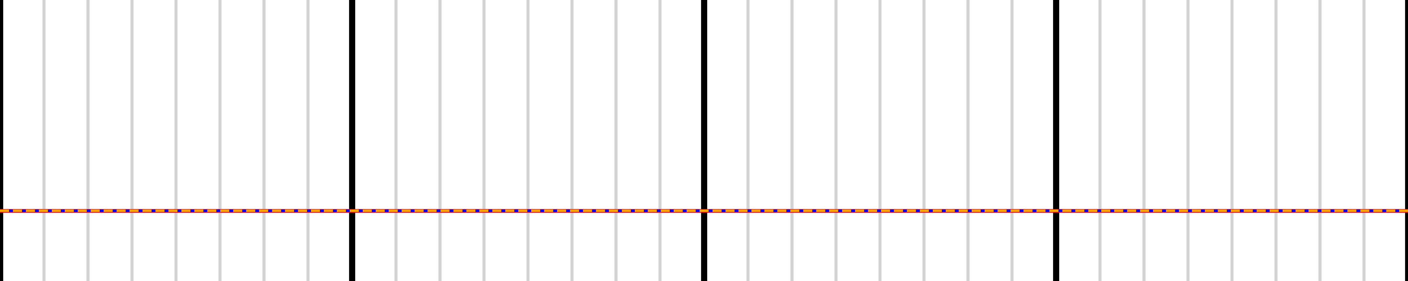
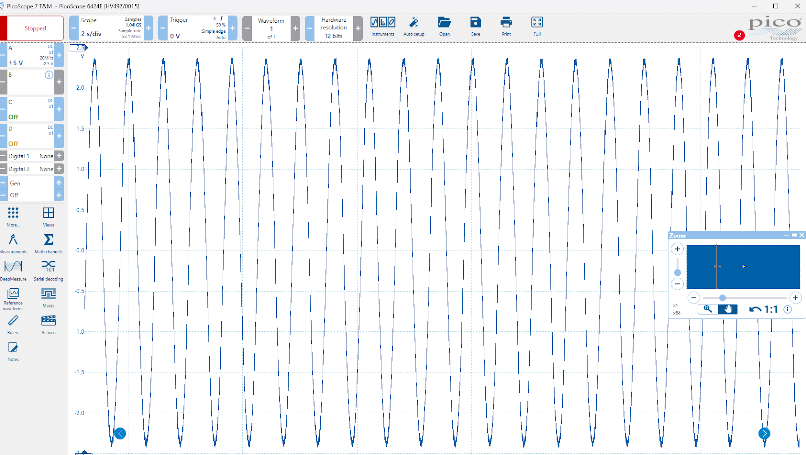
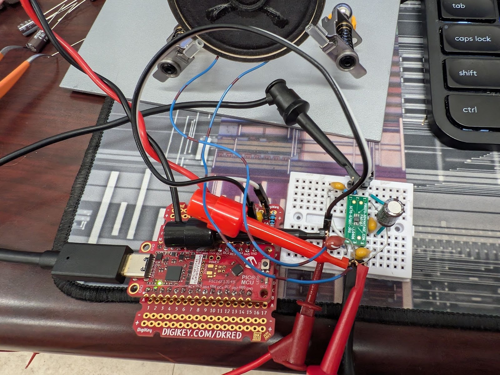
I filtered the DAC output externally with a simple RC filter. Here’s the analog output captured on a scope:
All you need to do to program it is to use the CLB1_SWIN_Write16 to write your DAC value.
Perfect for adding another DAC output for tuning, changing a setpoint etc. Complementing the existing DAC onboard and PWM by allowing for 6-8 more bits of resolution and/or additional. outputs.
Pairing it with a Microchip MIC920 op amp, I was able to stream audio from my PC to the board.
Discussion
The PIC16F13145 has a built-in DAC, as well as PWM. There are pros and cons to each, generally this CLB dac will outperform the PWM and internal DACs across speeds and performance. Unfortunately, due to limitations in the SWIN registers, the system is capped at approximately 100 ksps.
Tradeoffs
| CLB DAC | PWM DAC | R2R DAC | |
|---|---|---|---|
| Max Resolution | 16 bit | 10 bit | 8 bit |
| BW @ 8 bit output | 50,000 Hz (limited by SWIN) | 310 Hz (limited by filter) | 50,000 Hz (limited by settling time) |
| BW @ 10 bit output | 31,000 Hz (limited by filter) | 20 Hz (limited by filter) | N/A (cannot achieve) |
| BW @ 16 bit output | 480 Hz (limited by filter) | N/A (cannot achieve) | N/A (cannot achieve) |
| External Components | R/C | R/C | None |
| Pin Flexibility | Any Digital | Any Digital | 2 fixed |
Conclusion
The CLB opens the door to capabilities that were previously off-limits on this device family. By building a delta-sigma DAC entirely from LUTs, we achieve 16-bit output surpassing the performance of both the built-in DAC and PWM-based analog generation.
With zero extra silicon and only basic RC filtering, this design delivers high-resolution analog outputs suitable for everything from sensor biasing to streaming audio.
- Drop-in CLB bitstream for PIC16F13145
- Source code for the DAC driver
- Demo with serial input
PS; Closing Notes
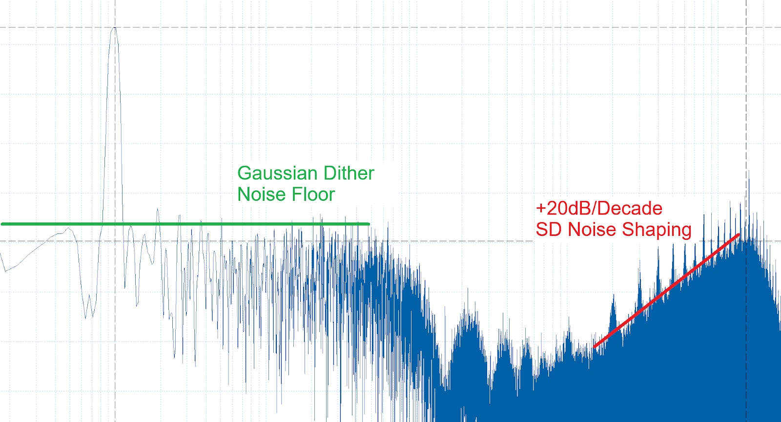
Here is a spectral density plot of the SD output before filtering during testing. This does not need dither for good time domain performance but it helps with SFDR etc.